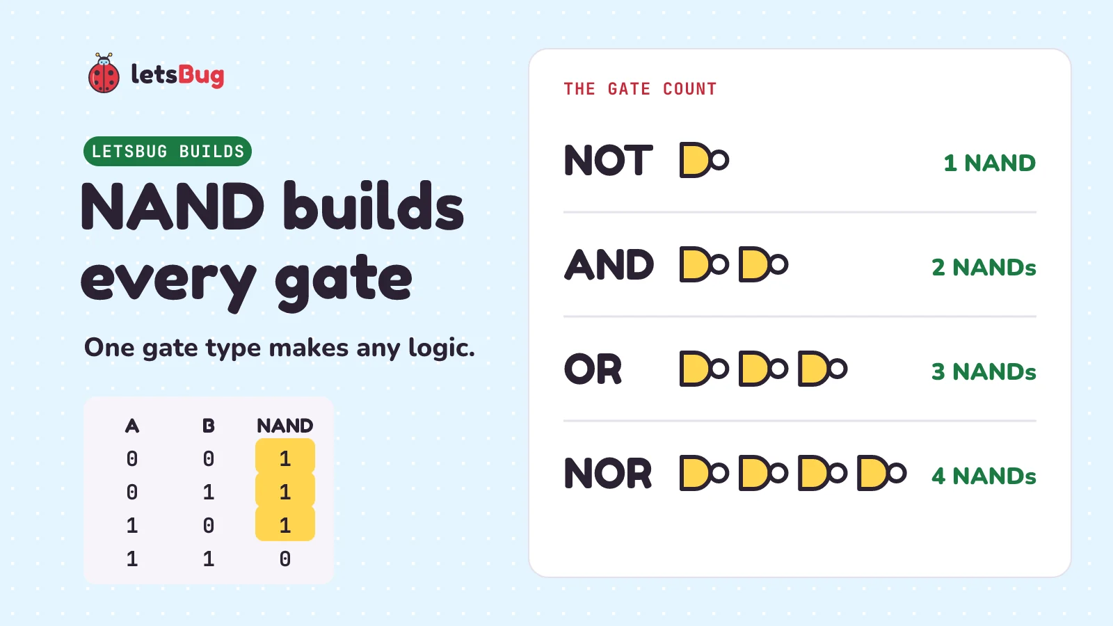
NAND is called a universal gate because NAND gates alone can build every other logic gate. Join a NAND's two inputs and it becomes NOT. Put that NOT after a second NAND and you get AND. Flip both inputs with two NANDs, and a third NAND gives OR. So one kind of part can make any logic circuit at all.
In this post, let's build NOT, AND, OR, NOR and XOR from NAND gates only. We'll check every truth table (the list of outputs for every pattern of inputs). We'll meet De Morgan's law, the trick that turns AND into OR. Then we'll count how many NANDs each gate needs, and see why chip makers like NAND. We'll also look at a computer that flew to the Moon, built mostly from one gate type. The NOT, AND and OR circuits open free in your browser.
Key takeaways
- A NAND gate (short for NOT AND) gives 0 only when both inputs are 1. Truth table (the output for A B = 00, 01, 10, 11): 1, 1, 1, 0.
- NOT = 1 NAND with its two inputs joined. AND = 2 NANDs: a NAND, then a NOT. OR = 3 NANDs: flip both inputs, then NAND. NOR = 4 NANDs: OR, then NOT.
- De Morgan's law: NOT (A AND B) is the same as (NOT A) OR (NOT B). That's why flipping both inputs of a NAND gives OR.
- A computer search over every small circuit shows these counts are the fewest possible. XOR also needs 4 NANDs, and XNOR needs 5.
- In CMOS, the way almost every chip is made, a NAND gate takes 4 transistors and an AND gate takes 6, because an AND is a NAND plus a NOT.
- The Apollo Guidance Computer that flew to the Moon used about 2,800 chips, mostly holding two NOR gates each. NOR is universal too.
- Never leave a gate input floating (connected to nothing). Join it to another input, or tie it to 0 or 1.
This post goes with letsBug Builds, episode 5. Watch it, or read on. Everything in the video is here. You also get the working in Python, the circuit text for the simulator, and practice questions with answers.
How do you make a NOR gate with transistors?
In the AND and OR gates using transistors post, two transistors in a row with a pull-up resistor gave NAND. (A pull-up resistor holds a wire at 1 until something pulls it down.) That episode's challenge was to put the two transistors side by side instead.
- Now either transistor can pull the middle wire down to 0.
- So the middle reads 1, 0, 0, 0. That's OR, flipped: NOR, short for NOT OR.
- Add the NOT gate after it, and the output reads 0, 1, 1, 1: OR again.
Keep NOR in mind. It's the gate the Apollo computer was built from, and we'll build it again below, this time from NANDs.
What is a NAND gate?
A logic gate is a tiny circuit that takes bits (0s and 1s) in and gives a bit out. From now on, we draw NAND as one symbol: the AND shape with a small circle on its output. That circle is called a bubble, and it means "flipped". It does the same job as last episode's stack of two transistors and its pull-up. But you don't need to see the transistors any more. You just need the rule:
The output is 0 only when both inputs are 1. Every other pattern gives 1.
| A | B | A NAND B |
|---|---|---|
| 0 | 0 | 1 |
| 0 | 1 | 1 |
| 1 | 0 | 1 |
| 1 | 1 | 0 |
You can buy NAND gates ready-made. Texas Instruments' SN74HC00 chip "contains four independent 2-input NAND Gates" in a 14-pin package (the plastic body with 14 metal legs). It runs on 2 V to 6 V. Its datasheet is the maker's list of a part's legs and limits. It has a function table, which is the chip's own truth table: H and H give L, and an L on either input gives H. (H means high, a 1. L means low, a 0.)
How do you make a NOT gate from a NAND gate?
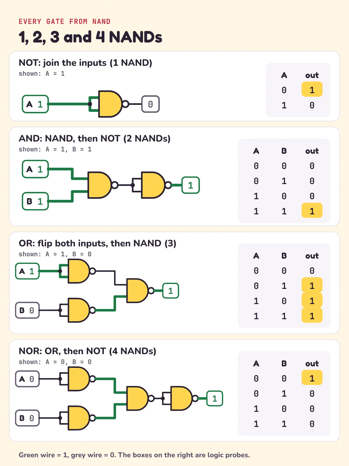
Join the NAND's two inputs together, so they always match. Wikipedia's NAND logic article says: "A NOT gate is made by joining the inputs of a NAND gate together."
Why does that work? With the inputs tied, only two rows of the NAND table can ever happen:
- 0 and 0, which gives 1.
- 1 and 1, which gives 0.
The output is always the opposite of the input. One NAND, and it's a NOT gate (also called an inverter).
How do you make an AND gate from NAND gates?
You built this in the last post: a NAND, then a NOT to flip it back. And that NOT is just another NAND with its inputs joined. So two NANDs make an AND: 0, 0, 0, 1.
- A and B both 1: the first NAND gives 0, and the NOT flips it to 1.
- Any other pattern: the first NAND gives 1, and the NOT makes it 0.
How do you make an OR gate from NAND gates?
This is the video's "pause and try". Flip both inputs first, using two NANDs as NOT gates. Then feed the flipped inputs into a third NAND. What does it give for all four patterns? Try it before you read on.
- A and B both 0: the flipped inputs are both 1, so the third NAND gives 0.
- Either input 1: at least one flipped input is 0, so the third NAND gives 1.
That's 0, 1, 1, 1: OR, from three NANDs. Here are all the gates so far in Python. Each new gate is built only from nand(), or from gates already built from it:
def nand(a, b):
    return 1 - (a & b)              # 0 only when both inputs are 1

def not_gate(a):
    return nand(a, a)               # 1 NAND: inputs joined

def and_gate(a, b):
    return not_gate(nand(a, b))     # 2 NANDs: NAND, then NOT

def or_gate(a, b):
    return nand(not_gate(a), not_gate(b))   # 3 NANDs: flip both inputs, then NAND

def nor_gate(a, b):
    return not_gate(or_gate(a, b))  # 4 NANDs: OR, then NOT

print("A B NAND NOT-A AND OR NOR")
for a in (0, 1):
    for b in (0, 1):
        print(a, b, nand(a, b), not_gate(a), and_gate(a, b), or_gate(a, b), nor_gate(a, b))
A B NAND NOT-A AND OR NOR
0 0 1 1 0 0 1
0 1 1 1 0 1 0
1 0 1 0 0 1 0
1 1 0 0 1 1 0(& is Python's AND for bits. Each gate's name ends in _gate because not, and and or are words Python already uses.)
What is De Morgan's law?
The OR trick has a name: De Morgan's law, named after Augustus De Morgan, a British mathematician of the 1800s. Wikipedia's De Morgan's laws article writes one of them like this: "not (A and B) = (not A) or (not B)".
In words: a NAND gate is the same as an OR gate whose inputs are flipped first. So if you flip the inputs before they reach a NAND, the two flips cancel out, and you're left with plain OR:
(NOT A) NAND (NOT B) = A OR B
Flip both inputs of an AND, flip its output too, and it turns into OR.
The Apollo Guidance Computer used De Morgan's law too. It could do OR, and it could flip bits, but it had no built-in way to do AND. So, in the words of Wikipedia's Apollo Guidance Computer article, "De Morgan's theorem was used to implement the equivalent of a logical AND." It did this by "inverting both operands, performing a logical OR through the bus, and then inverting the result." (Operands are the numbers being worked on, and the bus is the set of wires that carries them.)
How do you make NOR and XOR from NAND gates?
NOR is OR, flipped: 1 only when both inputs are 0. So build OR from three NANDs, then add one more NAND with its inputs joined, as a NOT. That's NOR from four NANDs: 1, 0, 0, 0.
XOR (exclusive OR) gives 1 when the inputs are different. It also takes four NANDs. The first NAND makes C = A NAND B. Two more make A NAND C and B NAND C. A fourth NAND joins those two, and the output is 0, 1, 1, 0. As the NAND logic article puts it, "An XOR gate is made by connecting four NAND gates". The trick is that the first NAND feeds two others.
XOR is next episode's gate, the one that adds two bits, as in how computers add numbers.
How many NAND gates does each gate need?
Here is the count for each gate:
| Gate | Built as | NANDs | Output for A B = 00, 01, 10, 11 |
|---|---|---|---|
| NOT A | A NAND A | 1 | 1, 1, 0, 0 |
| AND | NOT (A NAND B) | 2 | 0, 0, 0, 1 |
| OR | (NOT A) NAND (NOT B) | 3 | 0, 1, 1, 1 |
| NOR | NOT (A OR B) | 4 | 1, 0, 0, 0 |
| XOR | (A NAND C) NAND (B NAND C), with C = A NAND B | 4 | 0, 1, 1, 0 |
Can anyone do better than these counts? We can let a computer check. This program tries every circuit of 1 NAND gate, then every circuit of 2, and so on. Any wire, including an output from an earlier gate, can feed any new gate. It stops at the first size that makes the gate we want:
from itertools import product

rows = list(product((0, 1), repeat=2))    # A B = 00, 01, 10, 11
A = tuple(a for a, b in rows)             # A's column: (0, 0, 1, 1)
B = tuple(b for a, b in rows)             # B's column: (0, 1, 0, 1)

def nand_column(x, y):                    # one NAND gate, worked out for all four rows at once
    return tuple(1 - (p & q) for p, q in zip(x, y))

def fewest(target):
    circuits, gates = {frozenset({A, B})}, 0   # a circuit = the set of columns on its wires (a frozenset can sit inside a set)
    while not any(target in c for c in circuits):
        circuits = {c | {nand_column(x, y)} for c in circuits for x in c for y in c}
        gates += 1
    return gates

targets = {"NOT A": (1, 1, 0, 0), "AND": (0, 0, 0, 1), "OR": (0, 1, 1, 1),
           "NOR": (1, 0, 0, 0), "XOR": (0, 1, 1, 0), "XNOR": (1, 0, 0, 1)}
for name, column in targets.items():
    print(name, fewest(column))
NOT A 1
AND 2
OR 3
NOR 4
XOR 4
XNOR 5So 1, 2, 3 and 4 are the fewest possible. Nobody can build OR from two NANDs. (XNOR, exclusive NOR, is XOR flipped: 1 when the inputs match.)
Every extra gate costs space on the chip and a little time. In the SN74HC00 datasheet, one gate takes a typical 9 ns to respond at 4.5 V and 25 °C, and at most 18 ns. (A nanosecond, ns, is a billionth of a second. At 2 V it's slower: 45 ns typical.) The four-NAND XOR has three gates in a row from input to output. So, as Wikipedia puts it, it has "a propagation delay three times that of a single NAND gate". (Propagation delay is the time a change at the input takes to reach the output.) Fewer gates in a row means a faster circuit.
But the main point is still true. The NAND logic article also says: "it is possible to implement any Boolean function using just NAND gates". (A Boolean function is any rule that turns input bits into an output bit.) Henry M. Sheffer published the proof in 1913. This is called functional completeness, and a gate that has it is called a universal gate.
Why do chip makers like NAND gates?
Almost every chip is made with CMOS, a way of building gates from pairs of tiny transistors called MOSFETs. Wikipedia's CMOS article says that as of 2011, 99% of chips were made this way.
In CMOS, a NAND gate is small. It works like this:
- Two transistors in a row pull the output down to 0 when both inputs are 1, just like last episode's stack.
- Instead of a pull-up resistor, two more transistors side by side pull the output up to 1 when either input is 0.
That's 4 transistors. An AND gate is a NAND plus a NOT, so it takes 6. Wikipedia's AND gate article says: "transistors T1-T4 realize the NAND gate and transistors T5 and T6 the inverter." (Realize means make, and T1 to T6 are the labels in its drawing.) It adds: "The need for an inverter makes AND gates less efficient than NAND gates."
Where is NAND used in real life?
- Your phone's storage. It's called NAND flash, named after the gate. The flash memory article on Wikipedia: "In NAND flash, cells are connected in series, resembling a CMOS NAND gate." (In series means in a row, like our stack.) The same article says that on smartphones, NAND flash is used to store files.
- A 1-bit memory. The SN74HC00 datasheet lists an "S-R latch" as one of its uses. (S and R stand for set and reset.) A latch stores one bit. As the flip-flop article on Wikipedia puts it, an SR latch "can be constructed from a pair of cross-coupled NOR or NAND logic gates". (Cross-coupled means each gate's output feeds the other gate's input.) We used one to clean up a bouncing button in the switch debouncing post.
- The Apollo Guidance Computer. Apollo 11 launched on 16 July 1969, and this computer flew on board. Its logic was built from one gate type, copied again and again. Wikipedia: the version "used in the crewed flights" had "about 2,800 ICs, mostly dual three-input NOR gates". (An IC, or integrated circuit, is a chip. Dual means two gates on each chip.) One gate type was enough, because "NOR gates are universal logic gates from which any other gate can be made, though at the cost of using more gates." NOR is NAND's twin. The article also notes that NASA did the main navigation with big computers in Houston. So the onboard computer was a helper, not the main navigator.
- A free course that builds a computer. It's called From Nand to Tetris. Its first project says: "The only building blocks that you can use in this project are primitive Nand gates and the composite gates that you will gradually build on top of them." Twelve projects later, students have built a whole computer and its software, all the way up to an operating system.
Try it free in Falstad
Falstad is a free circuit simulator (a program that acts like a real circuit) that runs in your browser. It was made by Paul Falstad, with a JavaScript version by Iain Sharp. Both circuits from the video open with one click:
- NOT, AND and OR: every gate is a NAND, and all three share the same inputs, A and B.
- Challenge start: A NAND B and A OR B, built from NANDs, side by side.
How to use it:
- Click A or B to flip it between 0 and 1. Go through all four patterns and fill in the three truth tables yourself. Count the gates as you go: one, two, three.
- Green wires are at a positive voltage (a 1), and grey ones are at ground, the 0 V wire (a 0).
- The small 0 or 1 boxes are logic probes: testers that show 1 when the wire is at 2.5 V or more, and 0 below that.
- If a probe ever disagrees with your table, check which wire goes where. One wire in the wrong place gives a different gate.
If a link ever stops working, open the simulator and paste the text into File > Import From Text. NOT, AND and OR:
$ 1 0.000005 10.20027730826997 50 5 50 5e-11
L 160 112 112 112 2 0 false 3.3 0
x 96 104 106 104 0 24 A
L 160 400 112 400 2 0 false 3.3 0
x 96 392 106 392 0 24 B
151 320 64 416 64 0 2 0 3.3
M 416 64 464 64 6 2.5
x 488 72 538 72 0 20 NOT A
151 320 176 416 176 0 2 0 3.3
151 480 176 576 176 0 2 0 3.3
M 576 176 624 176 6 2.5
x 648 184 718 184 0 20 A AND B
151 320 272 416 272 0 2 0 3.3
151 320 368 416 368 0 2 0 3.3
151 480 320 576 320 0 2 0 3.3
M 576 320 624 320 6 2.5
x 648 328 708 328 0 20 A OR B
x 256 456 506 456 0 24 Every gate here is a NAND
w 160 112 208 112 0
w 208 48 208 80 0
w 208 80 208 112 0
w 208 112 208 160 0
w 208 160 208 256 0
w 208 256 208 288 0
w 160 400 240 400 0
w 240 192 240 352 0
w 240 352 240 384 0
w 240 384 240 400 0
w 208 48 320 48 0
w 208 80 320 80 0
w 208 160 320 160 0
w 240 192 320 192 0
w 416 176 448 176 0
w 448 160 448 176 0
w 448 176 448 192 0
w 448 160 480 160 0
w 448 192 480 192 0
w 208 256 320 256 0
w 208 288 320 288 0
w 240 352 320 352 0
w 240 384 320 384 0
w 416 272 448 272 0
w 448 272 448 304 0
w 448 304 480 304 0
w 416 368 448 368 0
w 448 368 448 336 0
w 448 336 480 336 0
And the challenge start:
$ 1 0.000005 10.20027730826997 50 5 50 5e-11
L 160 112 112 112 2 0 false 3.3 0
x 96 104 106 104 0 24 A
L 160 400 112 400 2 0 false 3.3 0
x 96 392 106 392 0 24 B
151 320 128 416 128 0 2 0 3.3
151 320 272 416 272 0 2 0 3.3
151 320 368 416 368 0 2 0 3.3
151 480 320 576 320 0 2 0 3.3
M 416 128 464 128 6 2.5
x 488 136 568 136 0 20 A NAND B
M 576 320 624 320 6 2.5
x 648 328 708 328 0 20 A OR B
x 176 472 596 472 0 20 Challenge - AND these two outputs together
w 160 112 208 112 0
w 208 112 208 256 0
w 208 256 208 288 0
w 160 400 240 400 0
w 240 144 240 352 0
w 240 352 240 384 0
w 240 384 240 400 0
w 208 112 320 112 0
w 240 144 320 144 0
w 208 256 320 256 0
w 208 288 320 288 0
w 240 352 320 352 0
w 240 384 320 384 0
w 416 272 448 272 0
w 448 272 448 304 0
w 448 304 480 304 0
w 416 368 448 368 0
w 448 368 448 336 0
w 448 336 480 336 0
Each line is one part. The new one is 151, a NAND gate: 2 is its number of inputs and 3.3 is the voltage it gives for a 1. Its two inputs sit 16 units above and below its left end, and its output is at its right end. L is a logic input (the box you click), M a logic probe, w a wire and x a text label.
What happens if you leave a NAND input floating?
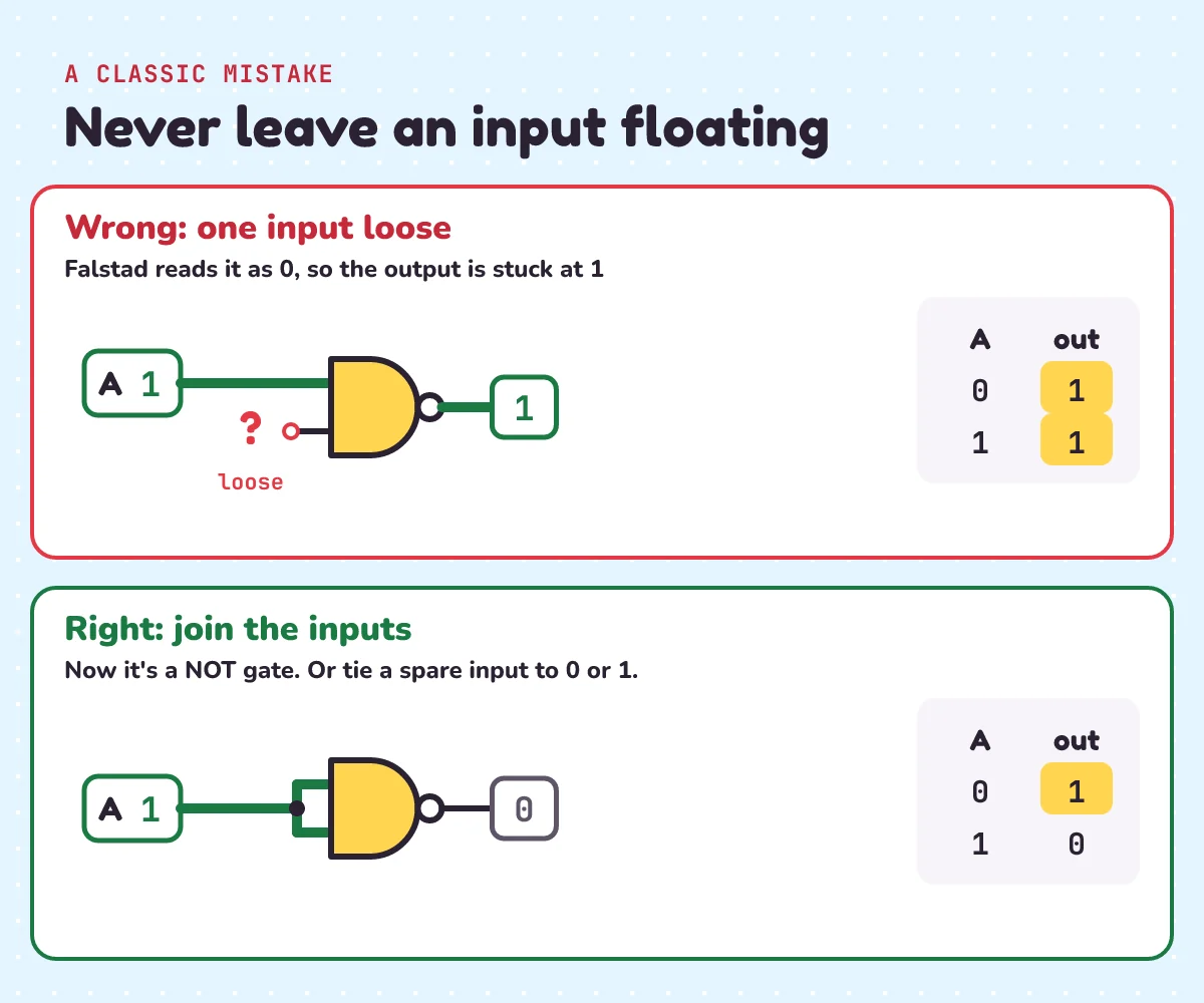
Here's a classic mistake. When you make a NOT gate, it's tempting to wire A to one input and leave the other one loose. A loose input, connected to nothing, is called floating.
In Falstad, a floating input reads as 0. Its source code connects any wire that touches nothing "to ground with a big resistor" (100 million ohms), so the wire sits at 0 V. With one input stuck at 0, the NAND's output is stuck at 1, whatever A does. In the episode's own test, the output stayed at 3.3 V for A = 0 and for A = 1.
On a real CMOS chip it's worse, because nothing holds a floating input at 0. It can drift to any voltage. Texas Instruments' note on floating CMOS inputs explains what happens when an input sits partway between 0 and 1, where the chip can't decide:
- Both of the input's transistors turn on at once. Then the supply current, the current the chip draws from its power supply, "can rise to several milliamperes per input". (A milliampere is a thousandth of an amp.)
- Also, "the outputs tend to oscillate", which means they flip back and forth between 0 and 1 on their own.
The SN74HC00 datasheet is just as clear: "inputs must not ever be left floating." So never leave an input floating. Join it to the other input, as in our NOT gate, or tie it to the supply (a 1) or to ground (a 0).
Practice questions
1) A NAND with both inputs joined gets a 1. What is the output?
2) How many NANDs make an OR gate?
3) A NAND gets A = 1 and B = 0. Then the same two inputs are flipped first, and fed to a NAND. What are the two outputs?
4) An SN74HC00 has four NAND gates. How many of them do you need to build one AND gate and one NOT gate?
5) The video's challenge: in the second Falstad circuit, add an AND gate (two more NANDs) that takes A NAND B and A OR B. What is its truth table? Which gate is it, and how many NANDs does this version use?
Show the answers
1) 0. Joined inputs make a NOT gate, and NOT 1 = 0.
2) Three: two NANDs as NOT gates flip the inputs, and a third NAND joins them.
3) 1 NAND 0 = 1. Flipped, the inputs are 0 and 1, and 0 NAND 1 = 1. The second one is 1 OR 0 = 1, by De Morgan's law.
4) AND takes 2 and NOT takes 1, so 3. One chip is enough, with 1 gate left over (tie its inputs to 0 or 1; never leave them floating).
5) It gives 0, 1, 1, 0: 1 only when the inputs are different. That's XOR, next episode's gate. This version uses 1 + 3 + 2 = 6 NANDs, but the fewest is 4. Using the gates from above:
xor = [and_gate(nand(a, b), or_gate(a, b)) for a in (0, 1) for b in (0, 1)]
print(xor)   # [0, 1, 1, 0]
Questions people ask
Why is NAND called a universal gate?
Because NAND gates alone can build every other logic gate: NOT from one NAND, AND from two, OR from three and NOR from four. With those, you can build any logic circuit at all. This property is called functional completeness, and Henry M. Sheffer published the proof in 1913.
How do you make a NOT gate from a NAND gate?
Join its two inputs together. Then only two input patterns can happen: 0 0, which gives 1, and 1 1, which gives 0. So the output is always the opposite of the input.
How many NAND gates make an OR gate?
Three. Two NANDs, each with its inputs joined, flip A and B. A third NAND takes the flipped inputs. By De Morgan's law, (NOT A) NAND (NOT B) = A OR B.
How many NAND gates make an XOR gate?
Four is the fewest. The first NAND makes C = A NAND B. Two more make A NAND C and B NAND C, and a fourth NAND joins those two. It has three gates in a row, so a change at the input takes three gate delays to reach the output.
Is NOR also a universal gate?
Yes. Like NAND, NOR alone can build every other gate. The Apollo Guidance Computer was built mostly from chips with two three-input NOR gates each.
Why are NAND gates used more than AND gates in chips?
In CMOS, a NAND gate takes 4 transistors, while an AND gate takes 6, because it is a NAND followed by a NOT gate. That makes AND gates less efficient than NAND gates.
What happens if a NAND input is left unconnected?
In Falstad, it reads as 0, so the output is stuck at 1. On a real CMOS chip, the input can drift between 0 and 1, draw extra current and make the output flip back and forth. Join it to another input, or tie it to 0 or 1.
Keep going
- Watch the full lesson, Why Is NAND a Universal Gate? Build Every Gate From NAND, or the Short, One Logic Gate Can Build Every Other Gate: NAND. More in the letsBug Builds series on YouTube.
- The episode before this one, where two transistors make AND, OR and NAND: AND gate and OR gate using transistors.
- Next, the XOR gate from the challenge, and how gates add: how do computers add numbers?
- Two NAND gates as a 1-bit memory that cleans up a bouncing button: switch debouncing.
Checked on 16 November 2026 against the 14 sources below. Every truth table and gate count in this post was worked out by a Python script, every Python sample was run, and both Falstad links were decoded, compared line by line with the circuit text above, and run through a small logic simulator for all four input patterns.
Sources
- Wikipedia: NAND logic (NOT, AND, OR, NOR and XOR from NAND; the CMOS NAND; Sheffer's 1913 proof; XOR's three gate delays)
- Wikipedia: Functional completeness (NAND and NOR are each functionally complete; universal gate)
- Wikipedia: De Morgan's laws (not (A and B) = (not A) or (not B); Augustus De Morgan)
- Wikipedia: Apollo Guidance Computer (about 2,800 ICs, mostly dual three-input NOR gates; AND done with De Morgan's theorem)
- Wikipedia: Apollo 11 (launched 16 July 1969)
- Wikipedia: AND gate (CMOS AND: NAND T1-T4 plus inverter T5 and T6)
- Wikipedia: CMOS (99% of IC chips made with CMOS as of 2011)
- Wikipedia: Flash memory (NAND flash cells in series, like a CMOS NAND gate; file storage on smartphones)
- Texas Instruments: SN74HC00 product page (four independent 2-input NAND gates, 2 V to 6 V)
- Texas Instruments: SNx4HC00 datasheet (14-pin packages; function table; propagation delay; S-R latch; inputs must not be left floating)
- Texas Instruments: Implications of Slow or Floating CMOS Inputs (SCBA004E) (supply current and oscillation with floating inputs)
- Wikipedia: Flip-flop (electronics) (an SR latch from two cross-coupled NAND gates stores one bit)
- Nand to Tetris: Project 1 and the course's 12 projects (build every gate from primitive Nand gates)
- Falstad: Circuit Simulator Applet and the circuitjs1 source (colours and clicking; the NAND gate element and its input positions; the 2.5 V probe threshold; unconnected wires tied to ground through a big resistor)