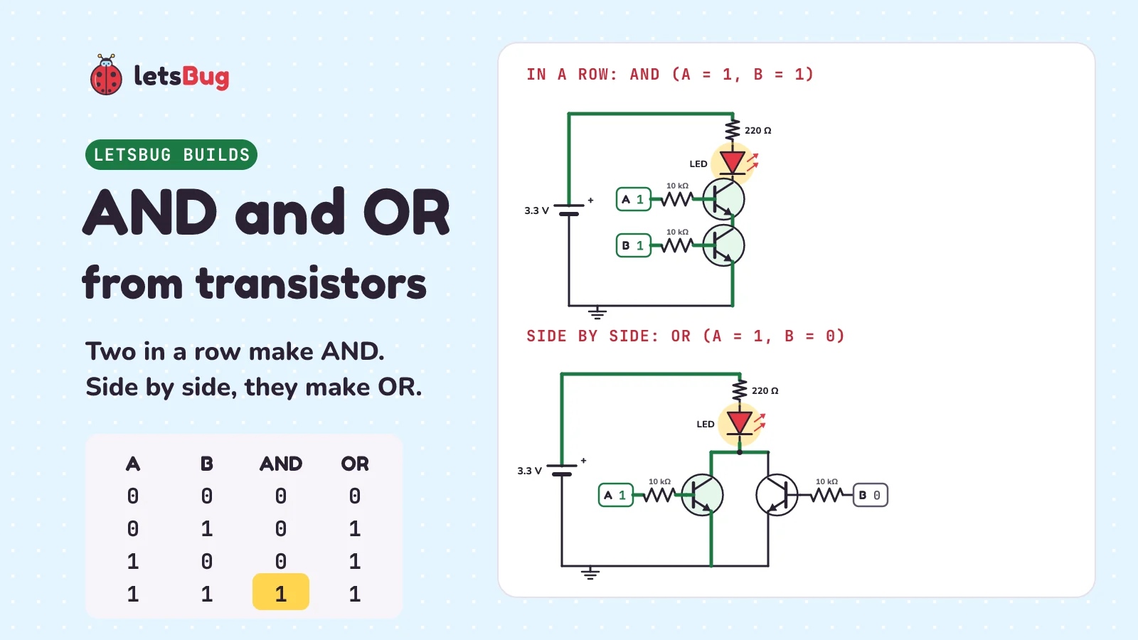
To make an AND gate using transistors (switches flipped by electricity), put two in a row. Current must pass through both, so an LED wired to them lights only when input A and input B are both 1. For an OR gate, put them side by side. Current can take either path, so one input at 1 is enough.
In this post, let's build both gates from 2N2222 transistors, test all four input patterns, and work out the LED current through the stack (the two transistors in a row) with Ohm's law (current = voltage ÷ resistance). Then we'll find the third gate hiding at the top of the stack, NAND (short for NOT AND), and turn it back into AND. You can click every circuit in a free browser simulator.
Key takeaways
- Two transistors in a row (one on top of the other, called a stack) make an AND gate: there's one path, so both must be on. Truth table (the output for A B = 00, 01, 10, 11): 0, 0, 0, 1.
- Two transistors side by side make an OR gate: there are two paths, so either one is enough. Truth table: 0, 1, 1, 1.
- Each input feeds its own base (the transistor's control leg) through a 10 kΩ resistor, so each base gets (3.3 V − 0.7 V) ÷ 10,000 Ω ≈ 0.26 mA (milliamps: thousandths of an amp).
- Through the stack, the LED gets (3.3 V − 1.9 V − 2 × 0.1 V) ÷ 220 Ω ≈ 5.5 mA, a little less than with one transistor.
- Take the output from the top of the stack with a pull-up resistor (one that ties the output to the supply, so it reads 1 until something pulls it down), and you get NAND (not AND): 1, 1, 1, 0. Add a NOT gate and it's AND again.
- In a CMOS chip (one built from pairs of tiny transistors called MOSFETs), the usual AND gate uses the same idea, NAND then NOT, with 6 transistors.
- Never wire A and B straight together. With one at 1 and the other at 0, the two pins try to hold one wire at two different voltages: a short circuit (a path with almost no resistance, so the current is far too big).
This post goes with letsBug Builds, episode 4. Watch it, or read on: everything in the video is here, plus the working in Python, the circuit text for the simulator, and practice questions with answers.
What happens when one NOT gate feeds another?
First, the challenge from the transistor as a switch post, where one transistor made a NOT gate: feed one NOT gate's output into a second NOT gate. Press the first gate's input button, and its output drops to 0. That turns the second transistor off, so the second output goes up to 1, and the second LED lights. Let go, and both flip back.
Two NOTs cancel out: NOT (NOT A) is just A. Remember that trick. We'll need it to turn NAND back into AND below.
What is a logic input in Falstad?
Our two inputs are called A and B. In Falstad, the free circuit simulator we use (a program that acts like a real circuit, in your browser), each one is a logic input: a small box you click to switch it between 0 V and 3.3 V. It does the job of last post's button and pull-down resistor (the resistor that held the base at 0 V while the button was up) in one part, with one difference. For a 0, it connects its wire straight to 0 V, with no resistor, just as it connects the wire straight to 3.3 V for a 1. An output pin on a chip does nearly the same: only its own tiny transistors sit between the wire and 0 V or the supply. That difference matters in the mistake near the end.
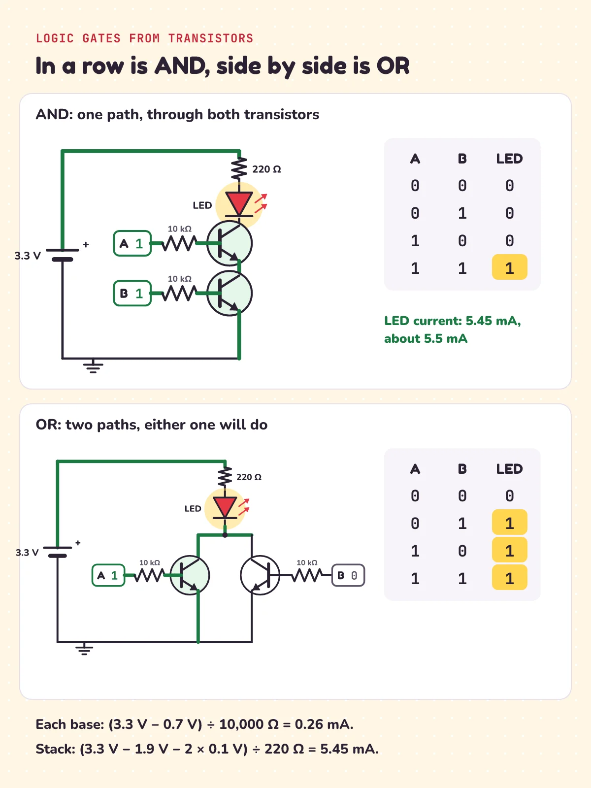
Each input feeds a transistor's base (its control leg) through its own 10 kΩ resistor (10,000 ohms). The base sits at about 0.7 V, so each base current is (3.3 V − 0.7 V) ÷ 10,000 Ω ≈ 0.26 mA, about a quarter of a milliamp, just like last time. Falstad showed between 0.257 mA and 0.272 mA.
How do you make an AND gate with transistors?
The LED and its 220 Ω resistor go down from the 3.3 V supply, as in the ESP32 LED blink post and the last post. Below them, two transistors stand in a row:
- The LED's bottom end goes into the top transistor's collector (where current goes in).
- The top transistor's emitter (where current comes out) goes into the bottom transistor's collector.
- Only the bottom transistor's emitter reaches ground (0 V).
Input A feeds the top transistor's base, and input B feeds the bottom one's.
So there's one path, and it goes through both transistors. Let's try the patterns:
- A on, B off: the bottom transistor blocks the path, so the LED is dark.
- A off, B on: the top one blocks it. Dark.
- Both on: current flows through both, and the LED lights.
With both on, the top transistor's base gets a little less current. Its emitter sits on the bottom transistor, about 0.1 V above ground, so its base sits at about 0.8 V: (3.3 V − 0.8 V) ÷ 10,000 Ω = 0.25 mA.
The LED is 1 only when A AND B are 1. That's an AND gate. The SN74HC08 is a chip with four AND gates. Its datasheet (the maker's list of a part's legs and limits) has a function table: the chip's own truth table. It gives the same rule: inputs H and H give H, and an L on either input gives L. (H means high, a 1, and L means low, a 0.)
How much current goes through the LED in a transistor AND gate?
Let's work it out, like the video's "pause and try". A transistor that's fully on still has about 0.1 V between its collector and emitter. In the stack, there are two of them. So:
- Start with 3.3 V.
- Take away 1.9 V for the red LED, and 2 × 0.1 V = 0.2 V for the two transistors.
- That leaves 3.3 V − 1.9 V − 0.2 V = 1.2 V across the 220 Ω resistor.
- Ohm's law (current = voltage ÷ resistance): 1.2 V ÷ 220 Ω ≈ 5.5 mA.
With one transistor, as in the last post, it was about 5.9 mA. So the stack gives a little less, because two transistors use up a little more voltage. Here's the same working in Python:
supply, v_led, v_ce, r_led = 3.3, 1.9, 0.1, 220   # volts, volts, volts, ohms
i_one = (supply - v_led - v_ce) / r_led            # one transistor (last post)
i_stack = (supply - v_led - 2 * v_ce) / r_led      # two in a row: two drops of 0.1 V
print(round(i_one * 1000, 1), "mA with one transistor")
print(round(i_stack * 1000, 2), "mA through the stack")
5.9 mA with one transistor
5.45 mA through the stackFalstad shows 5.84 mA. It's a bit more than our 5.45 mA, because Falstad's LED takes 1.84 V, not 1.9 V, and its transistors take 0.09 V each, not 0.1 V. Where does 0.1 V come from? The P2N2222A is onsemi's version of the 2N2222. Its datasheet promises a maximum of 0.3 V with a much bigger 150 mA flowing, and up to 1.0 V at 500 mA, so the drop grows with the current.
Those tests also push a big current into the base: 15 mA and 50 mA. The datasheet gives no number for a few milliamps like ours, so we checked in Falstad. Falstad's transistor is a general model, not this exact part, and it showed 0.09 V. So we use a round 0.1 V.
How do you make an OR gate with transistors?
Same supply, same LED and resistor. But now the two transistors stand side by side. Their collectors join under the LED, and both emitters go to ground. Now there are two paths:
- A on: current takes A's path, and the LED lights.
- B on: it takes B's path. Lit.
- Both on: both paths. Still lit.
- Both off: no path, so it's dark.
The LED is 1 if A OR B is 1. That's an OR gate. Or, as Wikipedia's OR gate article puts it: "It outputs a 1 if any of these inputs are 1, or outputs a 0 only if all inputs are 0." In Falstad, the LED current was 6.23 mA with one transistor on and 6.31 mA with both. The two transistors share the current, so each carries about half. A transistor carrying less current has a smaller drop across it, so the LED's resistor gets slightly more voltage.
Compare these tables with the switch tables in the what is a bit and a byte post (Builds episode 2), where two switches in series (in a row) made AND and two in parallel (side by side) made OR. They match exactly. These transistors are just switches flipped by electricity.
| A | B | In a row: A AND B | Side by side: A OR B |
|---|---|---|---|
| 0 | 0 | 0 | 0 |
| 0 | 1 | 0 | 1 |
| 1 | 0 | 0 | 1 |
| 1 | 1 | 1 | 1 |
Where are AND and OR gates used in real life?
- AND on a factory press. A power press is a machine that stamps metal with great force. In the US, OSHA, the government's workplace safety office, has a rule for presses called 29 CFR 1910.217. It says each of the two hand controls must be arranged "so that the concurrent use of both hands is required to trip the press". Concurrent means at the same time, and to trip the press means to start it. So both hands are on the buttons, away from the moving parts: left button AND right button.
- OR on your keyboard. Wikipedia's Shift key article says "There are typically two Shift keys", one on the left and one on the right. Hold the left Shift OR the right Shift while you press a letter, and you get a capital letter.
How do you make a NAND gate with transistors?
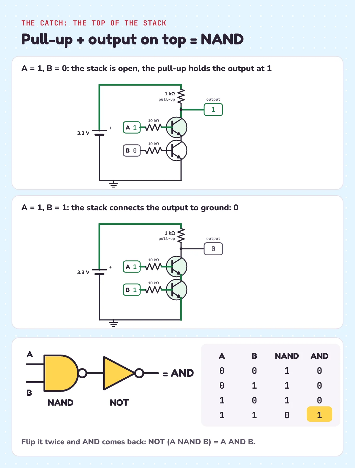
There's a problem. An LED is fine to light, but a gate's output should be a voltage that can feed the next gate. So let's swap the LED and its 220 Ω resistor for a 1 kΩ pull-up resistor: a resistor up to the supply that holds a wire high (a 1) until something pulls it down. Then take the output from the top of the stack (the top transistor's collector), just like the NOT gate in the last post.
- Both inputs 1: the stack connects the output to ground, so it's 0. In Falstad, it read 0.145 V.
- Any other pattern: at least one transistor is off, so there's no path through the stack. The pull-up holds the output high, so it's 1.
That gives 1, 1, 1, 0: AND, flipped. It's called NAND, short for NOT AND. Wikipedia's NAND gate article describes the same circuit with two switches: "If either of the switches S1 or S2 is open, the pull-up resistor R will set the output signal Q to 1 (high)." (S1 and S2 are the two switches, R is the pull-up, and Q is the output. An open switch has a gap, so it's off. A closed switch is on.)
And: "If S1 and S2 are both closed, the pull-up resistor will be overridden by the switches, and the output will be 0 (low)." Overridden means beaten: the closed switches win.
How high is the 1? In the second Falstad circuit below, the NAND output also feeds a NOT gate's base through a 10 kΩ resistor (more on that in the next section). So a small current flows through the pull-up: (3.3 V − 0.7 V) ÷ (1,000 Ω + 10,000 Ω) ≈ 0.24 mA. (The two resistors are in a row, so their ohms add up.) The pull-up drops 1,000 Ω × 0.24 mA ≈ 0.24 V, so the output sits at 3.3 V − 0.24 V ≈ 3.06 V. Falstad read 3.056 V.
How do you turn a NAND gate back into AND?
Use the trick from the start: flip it again. Feed the NAND output into a NOT gate, built like the last post's but without the pull-down: the NAND output always drives its input, so it is never left unconnected. Now the output is 0, 0, 0, 1. That's AND again, and this time the output is a voltage, not a lit LED: Falstad read 2.803 V for a 1 and 0.097 V for a 0. So it can feed the next gate's input.
Here are all four gates in Python. & is Python's AND for bits, and | is its OR:
def and_gate(a, b):
    return a & b              # in a row: both must be on

def or_gate(a, b):
    return a | b              # side by side: either one is enough

def nand_gate(a, b):
    return 1 - and_gate(a, b) # output from the top of the stack

def not_gate(a):
    return 1 - a

print("A B AND OR NAND NOT-NAND")
for a in (0, 1):
    for b in (0, 1):
        print(a, b, and_gate(a, b), or_gate(a, b), nand_gate(a, b), not_gate(nand_gate(a, b)))
A B AND OR NAND NOT-NAND
0 0 0 0 1 0
0 1 0 1 1 0
1 0 0 1 1 0
1 1 1 1 0 1The last column matches the AND column on every row: NAND followed by NOT is AND.
Real chips do the same. Many chips are made with CMOS: a way of building each gate from pairs of tiny transistors called MOSFETs, like the phone-chip inverter in the last post. Wikipedia's AND gate article says that in chip families like CMOS, "an AND gate is built from a NAND gate followed by an inverter". (An inverter is another name for a NOT gate.)
In its CMOS drawing, "transistors T1-T4 realize the NAND gate and transistors T5 and T6 the inverter": 6 transistors in all. (Realize means make, and T1 to T6 are the labels on the transistors in its drawing.)
You can buy them ready-made. Texas Instruments' SN74HC08 chip "contains four independent 2-input AND gates" in a 14-pin package (the plastic body with 14 legs). That's 4 gates × 2 inputs = 8 input pins, 4 output pins, and 2 pins for the supply and ground: 8 + 4 + 2 = 14. It runs on 2 V to 6 V, so 3.3 V is fine. For OR, the 74HC32 holds four 2-input OR gates.
To see what gates like these can do together, read how computers add numbers. Next in Builds: why chip makers often use the flipped gate. With NAND gates alone, you can build every other gate, a property called functional completeness.
Try it free in Falstad
Falstad was made by Paul Falstad, with a JavaScript version by Iain Sharp. Both circuits from the video open with one click:
- AND and OR: the AND (in a row) and the OR (side by side) next to each other.
- NAND, then NOT: the stack with its pull-up, feeding a NOT gate, with a logic probe (a small tester that shows 0 or 1) in the middle and one at the output, and an LED on the output.
How to use it:
- Click A or B to flip it between 0 and 1. Try all four patterns, and fill in both truth tables yourself.
- Green wires are at a positive voltage, grey ones are at ground, and the moving yellow dots are current.
- In the second circuit, the 0 or 1 boxes are logic probes: small testers that show 1 when the wire is at 2.5 V or more, and 0 below that. Watch the middle probe show NAND while the output shows AND.
If a link ever stops working, open the simulator and paste the text into File > Import From Text. AND and OR:
$ 1 0.000005 10.20027730826997 50 5 50 5e-11
v 96 464 96 112 0 0 40 3.3 0 0 0.5
w 96 112 400 112 0
r 400 112 400 176 0 220
162 400 176 400 240 0 1 0 0
w 400 240 400 272 0
t 352 288 400 288 0 1 0 0 100 default
w 400 304 400 336 0
t 352 352 400 352 0 1 0 0 100 default
w 400 368 400 464 0
w 96 464 400 464 0
g 96 464 96 496 0 0
L 208 288 160 288 2 0 false 3.3 0
r 208 288 352 288 0 10000
L 208 352 160 352 2 0 false 3.3 0
r 208 352 352 352 0 10000
x 130 280 150 280 0 24 A
x 130 344 150 344 0 24 B
x 150 530 400 530 0 24 AND (in a row)
v 576 464 576 112 0 0 40 3.3 0 0 0.5
w 576 112 880 112 0
r 880 112 880 176 0 220
162 880 176 880 240 0 1 0 0
w 880 240 880 320 0
w 880 240 960 240 0
w 960 240 960 320 0
t 832 336 880 336 0 1 0 0 100 default
t 1008 336 960 336 0 1 0 0 100 default
w 880 352 880 464 0
w 960 352 960 464 0
w 576 464 880 464 0
w 880 464 960 464 0
g 576 464 576 496 0 0
L 704 336 656 336 2 0 false 3.3 0
r 704 336 832 336 0 10000
L 1104 336 1152 336 2 0 false 3.3 0
r 1104 336 1008 336 0 10000
x 626 328 646 328 0 24 A
x 1166 328 1186 328 0 24 B
x 660 530 920 530 0 24 OR (side by side)
And NAND, then NOT:
$ 1 0.000005 10.20027730826997 50 5 50 5e-11
v 96 464 96 112 0 0 40 3.3 0 0 0.5
w 96 112 400 112 0
w 400 112 656 112 0
r 400 112 400 208 0 1000
w 400 208 400 272 0
t 352 288 400 288 0 1 0 0 100 default
w 400 304 400 336 0
t 352 352 400 352 0 1 0 0 100 default
w 400 368 400 464 0
L 208 288 160 288 2 0 false 3.3 0
r 208 288 352 288 0 10000
L 208 352 160 352 2 0 false 3.3 0
r 208 352 352 352 0 10000
w 400 208 480 208 0
M 480 208 480 160 6 2.5
w 480 208 480 288 0
r 480 288 608 288 0 10000
t 608 288 656 288 0 1 0 0 100 default
r 656 112 656 208 0 470
w 656 208 656 272 0
w 656 304 656 464 0
w 656 208 752 208 0
r 752 208 752 272 0 1000
162 752 272 752 336 0 1 0 0 0.002
w 752 336 752 464 0
M 752 208 816 208 6 2.5
w 96 464 400 464 0
w 400 464 656 464 0
w 656 464 752 464 0
g 96 464 96 496 0 0
x 130 280 150 280 0 24 A
x 130 344 150 344 0 24 B
x 500 184 580 184 0 20 NAND out
x 800 180 870 180 0 22 AND out
x 280 530 400 530 0 24 NAND
x 560 530 760 530 0 24 then NOT gives AND
Each line is one part, as in the last post. The new one is L, a logic input: the 2 makes it show 0 or 1, and 3.3 0 are its high and low voltages. t is a transistor, r a resistor in ohms, 162 an LED, M a logic probe, w a wire, g ground and x a text label.
Can you join two inputs together to make an OR gate?
Here's a common mistake. Building OR, it's tempting to save a transistor: join the A and B wires together and feed one base. Now set A to 1 and B to 0.
- A's pin tries to hold that wire at 3.3 V.
- B's pin tries to hold it at 0 V.
- Nothing sits between them, so it's a short circuit: a path with almost no resistance, pin to pin.
Falstad stops and shows "Path to ground with no resistance!" On a real board, nothing limits that current except the two pins themselves, so it can damage both of them. A and B are inputs to our gate, but each one comes from an output: Falstad's input box, or a pin (one of a chip's metal legs) on a real chip. So never wire two outputs straight together. Give each input its own transistor, as in our OR gate, or at least its own resistor, so something always sits between the two pins.
Real gate circuits keep their inputs apart too. Wikipedia's article on resistor-transistor logic (a way of building gates from resistors and transistors) describes a one-transistor gate with a separate base resistor for each input, and a version with "a set of parallel-connected transistor switches driven by the logic inputs". (Parallel-connected means side by side. Driven by the logic inputs means each input switches its own transistor.)
Practice questions
1) Two transistors in a row, A = 1, B = 0. Is the LED on?
2) The NAND output feeds a NOT gate. A = 1, B = 1. What is the final output?
3) Three transistors in a row, each with 0.1 V across it when on, a red LED (1.9 V) and 220 Ω on 3.3 V. With all three on, about how much current flows?
4) The SN74HC08 has four 2-input AND gates. How many of its 14 pins are inputs?
5) The video's challenge: in the second Falstad circuit, put the two input transistors side by side instead of in a row. What does the middle probe show for the four patterns, and what does the output show? Which gates are they?
Show the answers
1) No. B's transistor is off, so it blocks the only path.
2) The NAND output is 0, and the NOT flips it to 1. That's AND: 1 AND 1 = 1.
3) 3.3 V − 1.9 V − 3 × 0.1 V = 1.1 V, and 1.1 V ÷ 220 Ω = 5.0 mA.
4) 4 × 2 = 8. The other 6 are the 4 outputs, the supply and ground.
5) Side by side, either transistor pulls the middle down, so the middle probe shows 1, 0, 0, 0: that's NOR (not OR). The NOT flips it to 0, 1, 1, 1: that's OR. Using the gates from above:
nor = [1 - or_gate(a, b) for a in (0, 1) for b in (0, 1)]
print(nor, [not_gate(x) for x in nor])   # [1, 0, 0, 0] [0, 1, 1, 1]
Questions people ask
How do you make an AND gate using transistors?
Put two transistors in a row: the first one's emitter goes into the second one's collector, and only the second emitter goes to ground. Feed input A and input B to the two bases through their own resistors. Current has one path, through both, so the LED lights only when A and B are both 1.
How do you make an OR gate using transistors?
Put two transistors side by side: join their collectors under the LED, and connect both emitters to ground. Each input feeds its own base. Current has two paths, so the LED lights when A or B is 1, or both.
Why does the top of a transistor stack give NAND?
If you take the output from the top of the stack, with a pull-up resistor to the supply, the output is pulled to 0 only when both transistors are on. Every other time, the pull-up holds it at 1. That's 1, 1, 1, 0: NAND, the flipped AND.
What is a NAND gate?
NAND is short for NOT AND. Its output is 0 only when all its inputs are 1, and 1 for every other pattern. Add a NOT gate after it, and you get AND back.
How many transistors are in a CMOS AND gate?
Six in the usual design: a NAND gate (4 transistors) followed by an inverter, or NOT gate (2 transistors). Real chips can have more: TI's SN74HC08 datasheet lists buffered inputs, and a buffer is an extra stage made of more transistors.
Can you join two inputs together instead of using two transistors?
No. With one input at 1 and the other at 0, the two pins they come from try to hold one wire at two different voltages, with nothing between them. That's a short circuit, and on a real board it can damage both pins. Give each input its own transistor, or at least its own resistor.
Which chip has four AND gates?
The 74HC08, for example Texas Instruments' SN74HC08. It has four 2-input AND gates in a 14-pin package and runs on 2 V to 6 V. The 74HC32 is the OR version.
Keep going
- Watch the full lesson, AND Gate and OR Gate Using Transistors: Build Both in Your Browser, or the Short, Two Transistors in a Row Make AND. Side by Side, They Make OR. More in the letsBug Builds series on YouTube.
- The episode before this one, with the transistor as a switch and the one-transistor NOT gate: transistor as a switch: build a NOT gate.
- Builds episode 2, where switches in a row and side by side make AND and OR: what is a bit and a byte?
- From gates to arithmetic, with XOR and a half adder: how do computers add numbers?
Checked on 4 November 2026 against the 11 sources below. Every number in this post was checked with a Python script, every Python sample was run, and both Falstad links were decoded and compared, line by line, with the circuit text above.
Sources
- Wikipedia: AND gate (a CMOS AND gate is a NAND gate, T1-T4, followed by an inverter, T5 and T6)
- Wikipedia: OR gate (output 1 if any input is 1; the 74HC32, four 2-input OR gates)
- Wikipedia: NAND gate (NOT AND; two switches and a pull-up resistor; functional completeness)
- Wikipedia: Resistor-transistor logic (parallel-connected transistor switches, one per logic input)
- onsemi: P2N2222A datasheet (collector-emitter saturation voltage, at most 0.3 V at 150 mA)
- Texas Instruments: SN74HC08 product page (four independent 2-input AND gates, 2 V to 6 V)
- Texas Instruments: SNx4HC08 datasheet (14-pin packages; the AND function table; pin functions: 8 inputs, 4 outputs, ground and supply)
- Cornell LII: 29 CFR 1910.217, mechanical power presses (two-hand controls need the concurrent use of both hands)
- Wikipedia: Shift key (typically two Shift keys, used to type capital letters)
- Falstad: Circuit Simulator Applet (colours, clicking to switch, the JavaScript port by Iain Sharp)
- GitHub: circuitjs1 source (the logic input: low or high voltage, numeric flag 2; the "Path to ground with no resistance!" stop)